
Pilot line for low-cost SiC wafer to launch in 2016
On the eve of volume use of SiC power devices, there is an urgent need to lower the cost of SiC wafers, which is why the wafer production technology of Sicoxs Corp., a Tokyo-based venture company, is coming under the spotlight.
Aiming to establish a business based on the manufacture of low-cost SiC wafers, Sicoxs plans to build a pilot line within fiscal 2016 to manufacture SiC wafers, applying novel technology involving the bonding of polycrystalline and single crystalline wafers.
The company was founded in June 2012, primarily by SiC wafer engineers from Hoya. Kaga Electronics Co., Ltd, an electronic components trading firm, is supporting the venture.
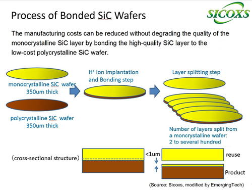
Sicoxs has achieved a low-cost wafer, less than half the cost of conventional SiC wafers, by bonding polycrystalline SiC and monocrystalline SiC wafers. Two wafers are directly bonded by argon (Ar) beam etching at room temperature.
Monocrystalline SiC wafer is quite expensive as the crystalline growth is dependent on the sublimation method. On the other hand, a polycrystalline wafer can be manufactured at relatively low cost. So Sicoxs' SiC wafer consists of a low-cost polycrystalline wafer as a support substrate and a thin monocrystalline SiC layer for device fabrication.
Bonded monocrystalline wafer can be split away* leaving a monocrystalline layer of the required thickness on the polycrystalline wafer, and can be reused. With this method, from two to several hundred layers can be split from one monocrystalline wafer to produce the same number of bonded SiC wafers. Including the cost of the polycrystalline wafer, the cost of the bonded SiC wafer will be less than half that of conventional SiC wafers.
*H+ ion is implanted at a depth corresponding to the desired thickness of the resulting monocrystalline layer before bonding and then annealing the bonded wafer splits the layer. The company reported that even with this process, the density of dislocations is similar to that of the original wafer.
Besides the bonding technology, polishing technology is another strength of the venture company. Polishing technology is indispensable for surface treatment before bonding and for the surface of the bonded monocrystalline layer.
Sicoxs was awarded a subsidy in June by the Japan Science and Technology Agency (JST). Sicoxs intends to use the subsidy to construct a production line capable of manufacturing wafers up to 6 inches in size and with annual capacity of several hundred thousand wafers. Plans call for the line to be completed within fiscal 2016.
The company is seeking a site for the production facilities in Japan. "We want to purchase all the equipment within the next fiscal year and start operation in fiscal 2016," said Motoki Kobayashi, general manager of Sicoxs' Technology Development Department.
Related articles:
SDK starts offering 6-inch SiC wafers (Nov. 12, 2013)
Air Water to offer 8-inch SiC and GaN wafers at low cost (May 24, 2013)
SDK expands SiC epiwafer production capacity 2.5 times (Aug. 31, 2012)
MHI bonds SiC and GaN with silicon wafer at room temperature (July 26, 2010)
Nippon Steel starts offering SiC wafers (Mar. 27, 2009)
The original article in Japanese appeared in the Aug. 6 issue of The Semiconductor Industry News. Translation by EmergingTech, which added the links and note.
Warning: Invalid argument supplied for foreach() in /home2/semicon/hosting/spiwww/include/Banner.php on line 78
Warning: array_multisort(): Argument #1 is expected to be an array or a sort flag in /home2/semicon/hosting/spiwww/include/Banner.php on line 81
Warning: Invalid argument supplied for foreach() in /home2/semicon/hosting/spiwww/include/Banner.php on line 85